Our ability to continuously shrink the features of our silicon-based processors appears to be a thing of the past, which has materials scientists considering ways to move beyond silicon. The top candidate is the carbon nanotube, which naturally comes in semiconducting forms, has fantastic electrical properties, and is extremely small. Unfortunately, it has proven extremely hard to grow the nanotubes where they're needed and just as difficult to manipulate them to place them in the right location. There has been some progress in working around these challenges, but the results have typically been shown in rather limited demonstrations.
Now, researchers have used carbon nanotubes to make a general purpose, RISC-V-compliant processor that handles 32-bit instructions and does 16-bit memory addressing. Performance is nothing to write home about, but the processor successfully executed a variation of the traditional programming demo, "Hello world!" It's an impressive bit of work, but not all of the researchers' solutions are likely to lead to high-performance processors.
We can work around that
There are many problems with carbon nanotubes. To begin with, while nanotubes naturally come in a semiconducting form, they're produced as a mixture of that process and the use of metallic nanotubes. While it's possible to purify the semiconducting versions, purity levels tend to plateau in the neighborhood of 99.9% purity. That's great for many situations, but when a processor will have millions of nanotubes, it's obviously not going to cut it. Nanotubes don't naturally form p- or n-type semiconductors (partial to conveying positive or negative charges, respectively). In silicon, these properties are driven by the addition of small amounts of an additional element, a process called doping. But nanotubes are so small that they're extremely difficult to dope.
Other issues come from the need to place the nanotubes in extremely precise locations to get any electronics to work. We haven't figured out how to get them to grow in any particular location, so scientists have had to make them separately and then let them settle onto surfaces. Unfortunately, this process generally creates a thin film of randomly oriented nanotubes, punctuated by aggregates where large numbers cluster up. And there will be a few randomly placed metallic nanotubes lurking within the film.
The new processor was made by a collaboration between MIT researchers and scientists at Analog Devices, Inc., who figured out a way to work around all of these issues.
The first workaround was to accept the chaos of nanotubes. Rather than trying to position a single tube at each location where it was needed, the researchers made a silicon surface with metallic features that were large enough to guarantee several nanotubes would typically bridge the gaps between the metal. To get rid of the aggregates, they deposited a layer of material on top of the nanotubes and then cracked it back off by sonication. The material took the aggregates with it, but it left the underlying layer of nanotubes undisturbed.
Next, to limit nanotubes to where they were needed, the researchers simply etched off most of the layer of nanotubes, leaving them only where they were wanted. They then added a variable layer of oxide on top of the nanotubes. The exact properties of the oxides, combined with different metals used to make connections, could convert the nanotubes into p- or n-type semiconductors as needed. While this process is more akin to doping an area that happens to contain nanotubes, it was effective at controlling the behavior of individual junctions.
And those metallic nanotubes still lurking in all of this? The researchers just left them in place and did a workaround in chip design.
Logical logic layout
While functional units of a chip do things like add two numbers, these units are built of collections of smaller logic gates that perform simple functions: NOT flips the value of a bit, logical AND takes a value of 1 if both of its input values are 1, and so on. There are often multiple ways of structuring these logic gates to form the same functional unit. So it might be possible to add two numbers using the right arrangement of five ANDs and seven NORs, it could also be done with six NOTs and four NANDs. (Note: those numbers are completely made up.)
The key insight by the researchers behind the new chip was that certain logical functions are less sensitive to metallic nanotubes than others. So they modified an open source RISC design tool to take this information into account. The result was a chip design that had none of the gates that were most sensitive to metallic carbon nanotubes.
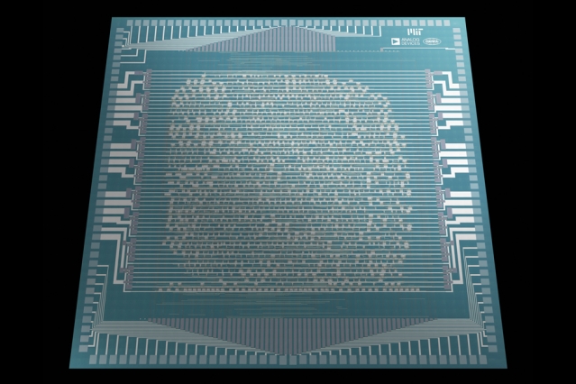
The resulting chip, which the team is calling the RV16X-NANO, was designed to handle the 32-bit-long instructions of the RISC-V architecture. Memory addressing was limited to 16-bits, and the functional units include instruction fetching, decoding, registers, execution units, and write back to memory. Overall, over 14,000 individual transistors were used for the RV16X-NANO, and the manipulations of the carbon nanotubes to make them resulted in a 100% yield. In other words, every single one of those 14,000 gates worked.
It was also what's considered a 3D chip, in that the metal contacts below the nanotube layer were used for routing signals among the different transistors, while a separate layer of metal contacts layered above the nanotubes was used to supply power within the chip.
Most critically, it works. As you can see from the image above, it successfully executed a variant of the traditional "Hello World" program that's generally used as a gentle introduction to the syntax of different programming languages.
Roadmap or detour?
In their paper, the researchers focus on all the ways their existing design could be improved. For example, the channel length is the distance between the metal contacts bridged by nanotubes. That length helps set the clockspeed, and for RV16X-NANO, the clockspeed was only 10kHz. The metal contacts also had to be very wide in order to ensure that there were enough nanotubes bridging them. We know in theory that improvements in both are possible, and ramping up the clockspeed is a definite option with this approach.
But because this design needs to tolerate metallic nanotubes (rather than getting rid of them), it's always going to need multiple nanotubes in each transistor. The design also needs to be wide enough that having a few nanotubes in bad orientations will still leave enough space for others to form functional contacts. And that means the features are necessarily going to be larger than we'd like and take longer to switch between states.
There also may be a cost in terms of total transistor count involved in working around the presence of metallic nanotubes through architecture, though that will probably vary depending on the purpose of a given functional unit.
These issues have varying prospects for being solved. There's nothing about this process that's preventing the gate length from shrinking, which would bring about clock speed increases; that's something researchers could try immediately. Some of the other issues would solve themselves if we could figure out a way of making a pure source of semiconducting nanotubes. That's obviously something people are working on, but this design will remain limited until that issue is solved.
But the ultimate goal here is to make single-nanotube transistors, which would require the ability to control the location of their placement on a chip. And there's nothing about this work that brings us any closer to that.
Overall, this is an impressive bit of engineering and an important validation that we can integrate carbon nanotubes with our existing chipmaking processes, as well as with the additional electronics that are necessary for a processor to function. But it doesn't go very far in terms of solving the issues that keep carbon nanotubes from reaching their full potential.
Nature, 2019. DOI: 10.1038/s41586-019-1493-8 (About DOIs).